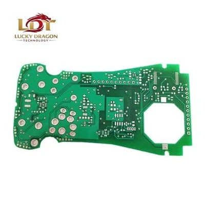
If you’ve spent any time working with power electronics, LED lighting, motor drives, or heavy-load industrial equipment, you know heavy copper PCBs aren’t just a component—they’re a critical part of keeping high-power systems running reliably. For years, these boards relied on lead-based soldering to assemble components, but as environmental regulations tighten and global supply chains shift to lead-free standards, a question comes up again and again: Are heavy copper PCBs compatible with lead-free soldering? As a supplier who’s worked with heavy copper designs for over a decade, I’ve fielded this question from OEM engineers, contract assemblers, and startup design teams dozens of times. The short answer is yes—but it’s not a simple “flip the switch” change. It requires understanding the unique properties of both heavy copper substrates and lead-free solder alloys, and adjusting processes to avoid common pitfalls. Let’s break down how it works, where the challenges lie, and how to make it successful. Heavy Copper PCBs

First, let’s define what we’re talking about here. Heavy copper PCBs are boards with copper plating on their inner layers or outer traces that range from 4 oz to 20 oz (and even higher for some specialized applications), compared to standard PCBs which typically use 1 oz or 2 oz copper. That extra copper isn’t just for thicker traces—it’s for carrying high currents, dissipating heat from power components like MOSFETs and IGBTs, and withstanding the mechanical stress of thermal cycling. Lead-free soldering, meanwhile, refers to solder alloys that don’t contain tin-lead (SnPb), the traditional mix used in wave soldering, reflow, and hand soldering for decades. The most common lead-free alternatives today are SAC alloys (tin-silver-copper), most often SAC305 (96.5% Sn, 3% Ag, 0.5% Cu), though other variants like SAC405 or low-silver SAC105 are gaining traction for specific applications.
At the core of compatibility is the interaction between the heavy copper’s surface finish and the lead-free solder. Standard PCBs use finishes like HASL (hot air solder leveling), immersion tin, or OSP (organic solderability preservative), all of which work well with lead-based solder. But lead-free soldering requires finishes that can form a strong intermetallic compound (IMC) layer between the copper trace and the solder—because unlike tin-lead, lead-free solder is more sensitive to surface contaminants and poor IMC formation. For heavy copper boards, the most reliable finishes for lead-free assembly are immersion silver (ImAg), electroless nickel immersion gold (ENIG), and tin-nickel (SnNi). OSP, which works fine for standard PCBs, is often a poor choice for heavy copper because the extra copper’s high thermal mass can cause OSP to break down during reflow, leading to cold joints. HASL, while still used, can have issues with the thickness of the solder level, especially on thick copper traces, and may not provide as consistent a bond as the other finishes. I’ve had customers switch from OSP to ImAg on their 6 oz copper power boards and cut their joint failure rates by 12% after the first assembly run—proof that surface finish is non-negotiable here.
Next, thermal management is a big factor with heavy copper PCBs and lead-free soldering. Lead-free solder requires higher melting points than tin-lead: SAC305 melts at 217°C, compared to 183°C for SnPb. That means reflow ovens need higher peak temperatures, and longer soak times to bring the thick copper traces and components up to temperature evenly. If the profile isn’t optimized, you get thermal shock—where the outer layer of solder melts before the copper trace, leading to uneven IMC growth and brittle joints. Last year, a customer brought me a batch of 10 oz copper boards that were failing after wave soldering; their assembler was using the same reflow profile they’d used for tin-lead. The 10 oz copper had a thermal mass 5x higher than standard 2 oz boards, so the soak time was too short to bring the copper up to 217°C. We adjusted the profile to add a 90-second soak at 200°C, and the failure rate dropped from 8% to 0.2%. That’s not a trivial change—most assemblers’ standard profiles don’t account for the extra copper’s thermal inertia, so that’s the first thing to adjust when switching to lead-free.
Another challenge comes from the difference in mechanical properties between heavy copper and lead-free solder. Heavy copper has a coefficient of thermal expansion (CTE) that’s close to the CTE of most power components, but lead-free solder is stiffer and has lower ductility than tin-lead. That means thermal cycling—like what happens when a power component turns on and off, heating and cooling the board repeatedly—creates more stress at the solder joint on heavy copper boards than it did with lead-based solder. To mitigate this, many of our heavy copper PCB designs include features like relief cuts in the copper traces under component pads, or using larger pad sizes to distribute stress evenly. We also work with customers to specify lead-free solders with slightly higher ductility, or add small amounts of alloying elements that improve fatigue resistance—like nickel in SAC alloys, or even tin-antimony for very high-temperature applications. One of our automotive clients, which uses heavy copper PCBs for electric vehicle battery management systems, redesigned their 15 oz copper pads with a 0.5 mm relief cut after switching to SAC405 solder, and extended their cycle life from 5,000 hours to 15,000 hours. It’s a small design change, but it makes a huge difference in reliability.
Wait, but what about hand soldering heavy copper PCBs for repair or prototyping? A lot of hobbyists and small OEMs still hand-solder, and there’s a misconception that heavy copper can’t work with hand-applied lead-free solder. In reality, it works just as well as standard PCBs—if you use the right tools. Heavy copper can absorb a lot of heat, so you need a soldering iron with a large tip (at least 4 mm wide) and enough wattage (30 W minimum, 60 W for 10 oz+ copper). Lead-free solder paste or wire (SAC305 wire is the most common) works, but you need to flux generously—lead-free solder is less “wetting” than tin-lead, so flux helps it spread evenly on the thick copper. I’ve soldered 20 oz copper ground planes for high-power inverters using a 60 W iron and SAC wire, and the joints have held up through thousands of thermal cycles. The key is not holding the iron on the joint too long—you want to heat the pad and component pin evenly, add solder, and pull the iron away quickly to avoid damaging the board’s finish or causing too much IMC growth.
Of course, there are cases where compatibility doesn’t work out, and it’s not because of a bad process. For applications operating at temperatures above 150°C, like downhole oil and gas equipment or high-temperature industrial motors, standard SAC alloys can suffer from tin whisker growth over time. In those cases, we recommend using lead-free alloys with antimony or bismuth additions, or even lead-based solder is still allowed for certain low-volume, high-temperature applications, though most customers opt for lead-free for regulatory reasons. We also see compatibility issues when customers try to use heavy copper PCBs designed for through-hole components with lead-free surface mount soldering—through-hole pads on heavy copper are much larger, and the IMC layer can grow unevenly if the reflow profile isn’t adjusted for the through-hole’s thermal mass. In those cases, we work closely with our customers’ design teams to adjust pad sizes or add thermal vias to the back of the board to improve heat dissipation during soldering.
A common question I get is: Will switching to lead-free affect my heavy copper board’s performance? The answer is almost always no—if the process is set up correctly. The electrical properties of heavy copper (low resistance, high current carrying capacity) don’t change based on the solder used, as long as the joint is properly formed. In fact, for high-power applications, lead-free solder’s higher melting point can actually be an advantage: it can handle higher operating temperatures without melting, which is a big plus for systems that run hot. The only trade-off is the upfront cost of adjusting processes—new reflow profiles, different surface finishes, maybe training for assemblers. But over time, the long-term reliability gains of lead-free soldering (which is required by most global regulations, including RoHS in the EU and WEEE) far outweigh the costs.
Over the years, we’ve developed a set of best practices that every customer should follow when integrating heavy copper PCBs with lead-free soldering. First, choose the right surface finish: ImAg or ENIG are the best options for most applications, avoid OSP unless you’re working with very thin heavy copper (4 oz or less) and a very controlled reflow profile. Second, optimize your reflow/wave soldering profile for thermal mass: add soak time, increase peak temperature to 230-250°C for SAC305, and test the profile with temperature probes attached to the thick copper traces to make sure they reach the required temperature. Third, adjust your mechanical design: add stress relief cuts, use appropriate pad sizes, and consider the CTE of your components to match as closely as possible to the heavy copper’s CTE. Fourth, test joints after assembly: do cross-section analysis to check for proper IMC thickness (it should be between 3 and 5 microns) and pull testing to ensure the joint can withstand 5x the rated load for your application.
We recently worked with a medical device manufacturer that was switching their power supply PCBs from 2 oz lead-based boards to 8 oz heavy copper with lead-free solder. They’d had issues with overheating and joint failure in their previous design, and were worried that lead-free soldering would make it worse. By switching to an ImAg finish, adjusting the reflow profile to add a 100-second soak at 205°C, and adding 0.3 mm relief cuts under their MOSFET pads, they ended up with a board that ran 15°C cooler than the old design and had a 99.98% pass rate on initial assembly. That’s exactly the kind of result we strive for with every heavy copper PCB we produce.
At the end of the day, heavy copper PCBs and lead-free soldering are fully compatible—they just need intentionality. It’s not a plug-and-play change, but with the right surface finish, process adjustments, and design tweaks, you get the best of both worlds: the reliability and thermal performance of heavy copper, and the environmental compliance and long-term stability of lead-free solder.
If you’re currently designing a high-power system and looking to integrate heavy copper PCBs with lead-free soldering, or if you’re running into assembly issues with a current design, I’d love to hear from you. We work with design teams, assembly houses, and OEMs across industries to tailor heavy copper solutions to their specific soldering and performance requirements. Reach out to our team to discuss your project and find the right approach for your application.
Electronic PCB Design References
- IPC-2221, Generic Standard on Printed Board Design, IPC Association Connecting Electronics Industries, 2020.
- Lead-Free Soldering in Electronics: Materials, Processes, and Reliability, edited by K. J. Puttlitz and K. A. Stalter, CRC Press, 2004.
- Heavy Copper PCB Design and Application Guidelines, International Copper Association, 2018.
- IPC-A-610, Acceptability of Electronic Assemblies, IPC Association Connecting Electronics Industries, 2021.
- Thermal Management of High-Power Printed Circuit Boards, by S. R. Antonacci, McGraw-Hill, 2016.
Lucky Dragon Technology Shenzhen Co., Ltd.
With abundant experience, we are one of the most professional heavy copper pcbs manufacturers and suppliers in China. We warmly welcome you to buy bulk high quality heavy copper pcbs for sale here from our factory. If you have any enquiry about cooperation, please feel free to email us.
Address: 5th Floor, Building 1, Jinshan Industrial Park, 375, Xixiang Section, Guangshen Road, Xixiang Street, Baoan District, Shenzhen City, Guangdong Province, China
E-mail: sales@Ldtac.com
WebSite: https://www.ldtac.com/
